
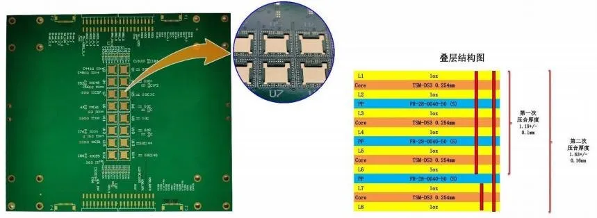
77 GHz radar high-frequency board
- Layers
- 18
- Materials
- TSM-DS3 + FR28 prepreg + S1000-2M, hybrid lamination
- Finish
- Immersion gold (ENIG)
- Special process
- Pure PTFE blind/buried-via impedance board, 5 back-drill groups
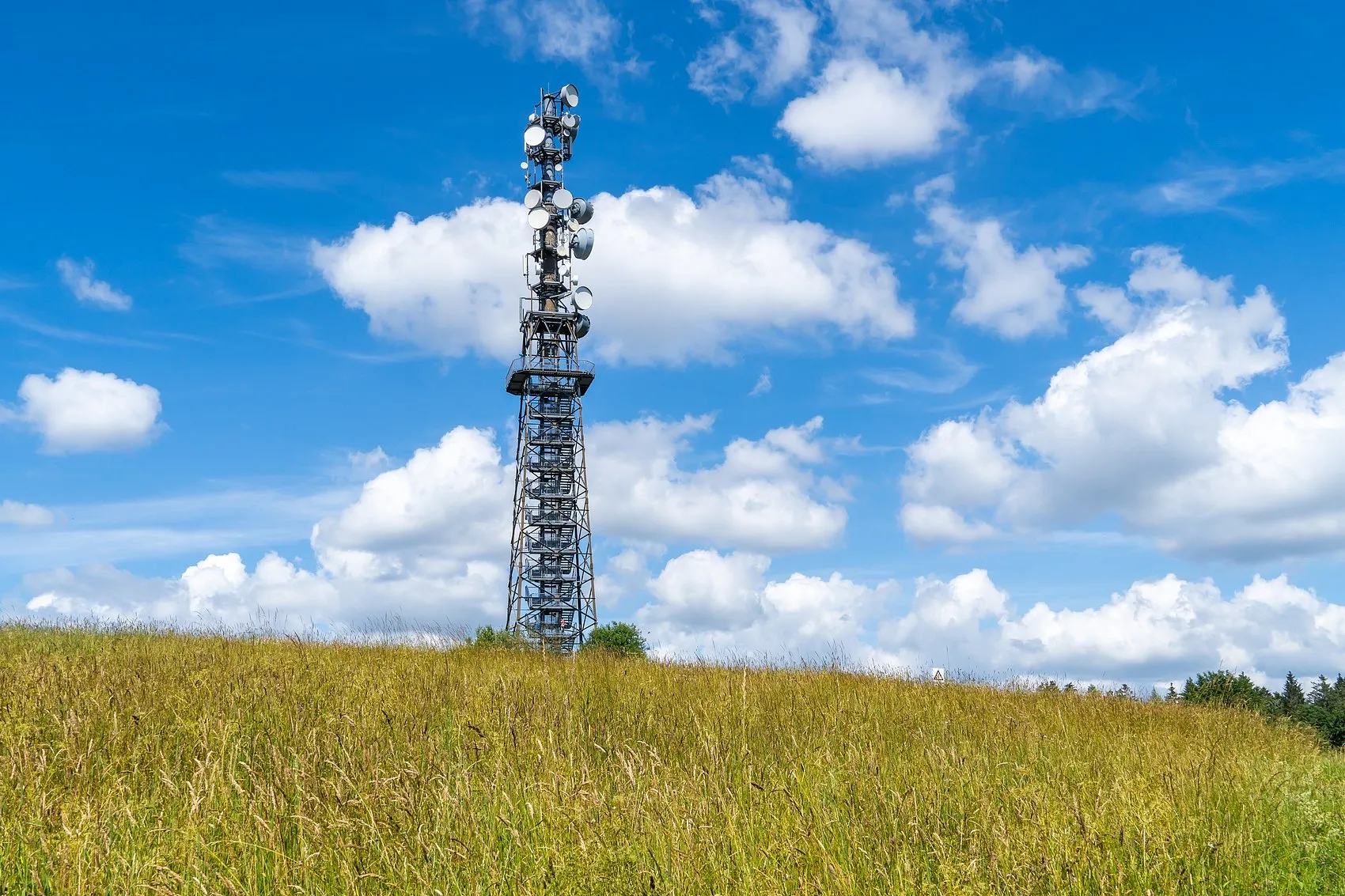
PCB and PCBA for communication equipment that combines RF sections with high-speed digital layers.
Telecom hardware often needs RF and low-loss materials, controlled impedance and back drilling. Hybrid stack-ups are reviewed per design. This describes typical requirements and is not a customer reference.
| Positioning | RF / Communication |
|---|---|
| Typical applications | 5G Base Stations, Routing & Switching, Optical Modules |
Source: ShinePCB capability workbook, navigation overview. Values are confirmed against your files and the assigned facility during engineering review; certificates are available on request.
Typical requirements from the ShinePCB application capability sheet. Each project is reviewed against its own drawing and specification.
| End product / typical modules | Applicable PCB types | Key processes | Material direction | Engineering focus |
|---|---|---|---|---|
| 5G base station AAU / BBU / RRU — antenna, RF front end, baseband, clock, power | Hybrid high-frequency, high-speed multilayer, HDI, heavy copper | Hybrid lamination; impedance; back drilling; high layer count; press-fit holes; heavy copper | Rogers / Taconic; ultra-low-loss | Phase / impedance consistency; high-speed links; heat dissipation |
| Routers / switches / servers / storage — main board, switch board, backplane | High-speed multilayer, high-layer-count backplane, HDI, heavy copper | High-speed impedance; back drilling; press-fit holes; low-loss lamination | MEGTRON / Isola / TUC low-loss | 112G/224G links; insertion loss; crosstalk; warpage |
| Optical modules / CPO — DSP, driver/TIA, flex interconnect | HDI, high-speed multilayer, FPC, rigid-flex, ceramic | Ultra-fine lines; laser vias; via-in-pad; impedance; thin boards | Ultra-low-loss; LCP / FPC; ceramic | Low loss; miniaturization; thermal management; cleanliness |
Application descriptions show typical board requirements. They are not customer references, and end-product standards remain the responsibility of the product owner. TL9000 is not held; telecom quality clauses are reviewed per project.
Board constructions from the ShinePCB company presentation — not customer references.
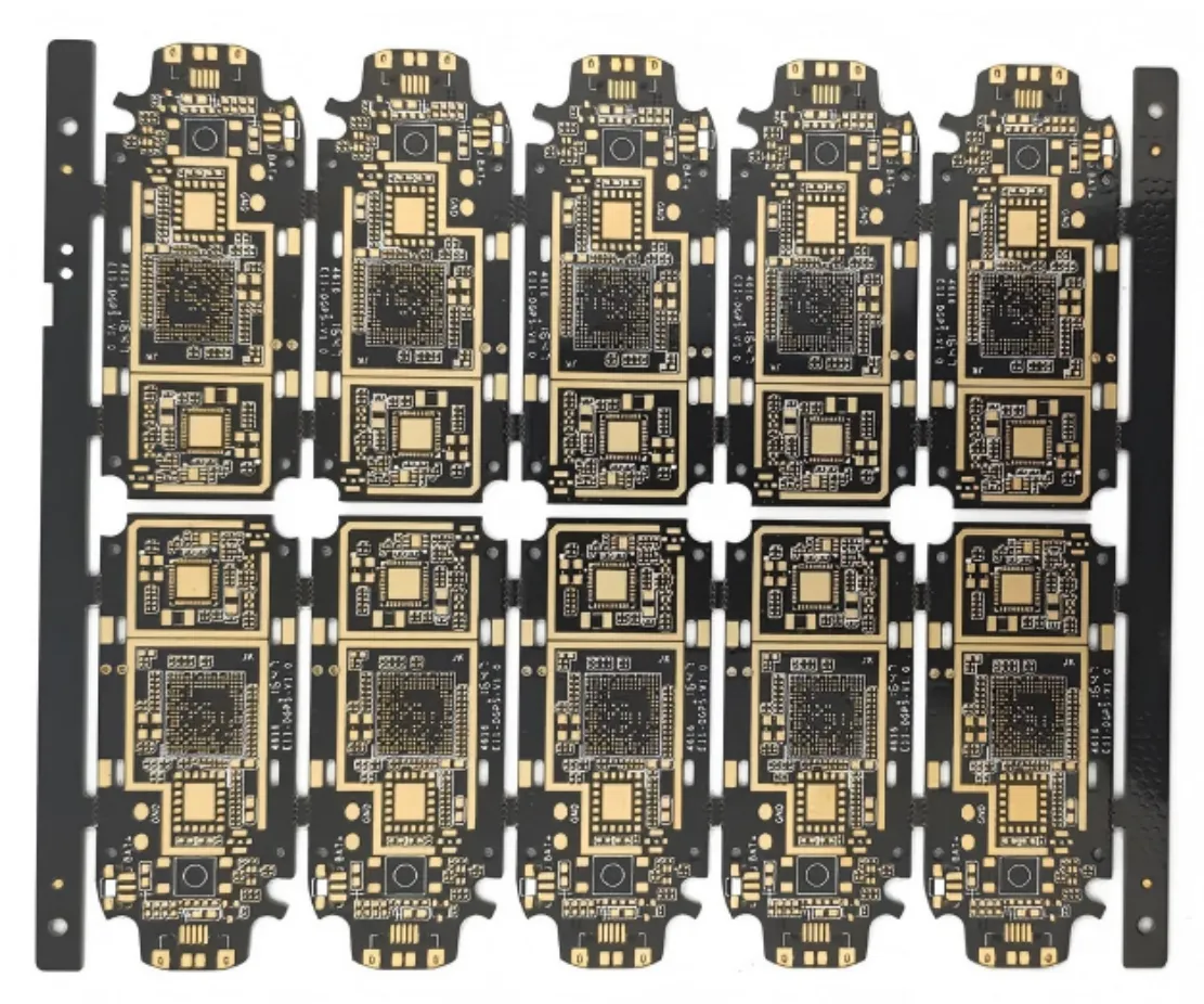
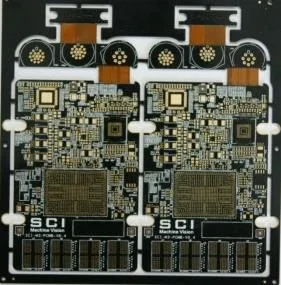
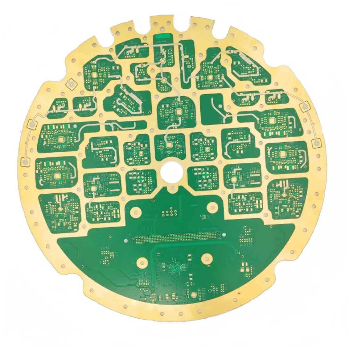
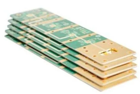
Builds from the ShinePCB company presentation. They illustrate process scope and are not customer references.
Hybrid stack-ups are reviewed per design.
Yes. See backplane PCB.